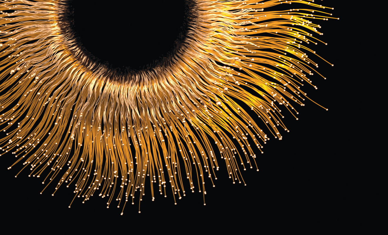
Offering equipment, space, and expertise, LEAP’s dedicated area in WPI’s Gateway Park serves as an innovation sandbox where researchers have the tools needed to push the boundaries of science, business partnerships bring ideas to market, and educators prepare a technical workforce ready to scale up the innovative materials as these developing technologies progress.
Most of us already use some form of photonics every day. Think of using a remote to change a television channel across the room, connecting to the internet using fiber-optic cables, or having laser eye surgery.
But this technology—which uses photons (light) guided through glass pipes rather than electrons guided through wires to enable faster, smaller, and less costly ways to transfer information—has potential that’s almost otherworldly. Integrated photonics applications could someday help your phone sense if you have diabetes long before an appointment with a physician confirms it. Or it may lead to a smaller endoscope that could diagnose abnormalities in a manner that today’s available technology simply can’t.
At WPI, all those futuristic possibilities are potential reality at the Lab for Education & Application Prototypes (LEAP@WPI/QCC).
A government-backed research and development partnership between WPI and Quinsigamond Community College (QCC), LEAP@WPI/QCC combines photonics education, application, and workforce development into a one-stop shop that blends the strengths of each institution and works within a developing ecosystem to build a foundation for this emerging technology to take off.
Integrated Photonics in a Nutshell
Photonics and optics researchers study the science of light and how it behaves and interacts with the world. Integrated photonics, which places photonic and optical components onto an integrated circuit that serves as building blocks for photonic integrated circuits (PIC), is just beginning to be parlayed into advanced research, says LEAP director Doug Petkie, department head and professor of physics at WPI. Right now, advances in developing photonics technology and investment on the local, state, and federal level are bringing this science to the forefront.
Integrated photonics is multidisciplinary in nature, so the potential impact for industries from communications to medical to military is broad and only barely imagined, let alone discovered, says Petkie. But it also requires an overhaul in thinking and infrastructure for a technology that’s not widely used or understood—yet.
Photonics and electronics currently operate on separate systems, so while future years might find photonics dominant, the in-between technology places photonics and electronics on one chip—called integrated photonics—and it’s the sweet spot for LEAP.
The idea is to create a network for advanced technology and create a workforce to support the manufacturing and research.
Doug Petkie
To get to the next step of bringing radical ideas to existence, critical government backing is seeding an ecosystem of LEAP facilities. The American Institute for Manufacturing Integrated Photonics (AIM Photonics) is one of 16 advanced manufacturing institutes included in the national Manufacturing USA initiative. Boosted by Mass. Manufacturing Innovation Initiative funding (in which the state matches federal funds), Massachusetts now has a growing constellation of LEAP facilities that includes MIT, Bridgewater State University, Stonehill College, and Western New England College (LEAP@WPI/QCC is the second established LEAP in the state). Each facility has a specialty, ranging from telecom and data (internet), light detection and ranging (radar), sensing (food safety, military), and microwave photonics technology (5G and 6G technologies).
“The idea is to create a network for advanced technology and create a workforce to support the manufacturing and research,” says Petkie. “WPI’s expertise in chemical and biological sensing, and some overlaps in microwave photonics and PIC sensing, will guide much of the work here.”
Manufacturing Trajectory
The multi-industry benefits of photonics are similar to Worcester’s earliest manufacturing successes with the production of tinware, textiles, and wire products. From developing a technically proficient manufacturing workforce on an emergent technology to harnessing the innovative ideas of industry leaders who will advance the use of photonics, LEAP positions WPI at the center of this developing technology.
Fitted with expensive, state-of-the-art equipment that is prohibitive for many companies to acquire or individuals to access on their own—such as a nanoscale 3D printer for prototyping or a probe machine for noninvasive optical metrology for reliability testing—the LEAP@WPI/QCC facility provides opportunity found in few other places. The space serves as a research lab, project classroom, industry sandbox, and real-world toolkit for education, research, and training. Testing and research potential also includes fiber optics, fiber-chip interfacing for integrated photonics, terahertz sensing, and optical and electrical device characterization.
James Eakin, senior technical operations manager at LEAP, says some of LEAP’s potential innovations will change the most basic ways we go about our lives. Someday the need for a traditional computer displays could even disappear, as augmented- and virtual-reality technologies emerge. Another example is photonics-based 6G “wallpaper” that acts like an invisible and large antenna to route connectivity and transfer information. Photonics also plays a role in improved personal safety as military personnel could wear clothing with embedded sensors to detect minute amounts of dangerous chemicals in the air.
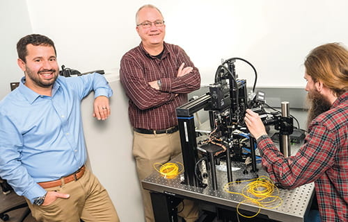
James Eakin, Doug Petkie and Jake Bouchard ’17, MS ’20
With developments from each industry collaboration, a domino effect will spill over into other industries, Petkie says, with reduced environmental impact being especially evident. When communications and data transfer moves to a photonics-based process, the footprint of sprawling data centers—now required for moving volumes of data and communications—will be drastically reduced even as their data output rises dramatically.
WPI’s rich resources and expertise in manufacturing, physics, electrical and computer engineering, and materials science overlaps in the projects to see how photonics interacts with different materials, in diverse settings, and with various components. This kind of multidisciplinary collaboration is key to bringing photonics possibilities to the broadest use.
QCC Collaboration and Workforce Development
To reach its full potential, photonics requires researchers who can uncover the best applications for the technology, educational opportunities in photonics science, facilities and equipment to produce and work with components, industries that can put photonics applications to real-world use in processes and products, and a trained workforce that can manufacture the tiny components needed throughout the process.
“There’s a lot still in flux,” says Adrienne Linnell, QCC’s program administrator for STEM Initiatives. “We need the technicians for jobs with integrated photonics, and we need PhDs doing research to develop the products and systems that will require integrated photonics. And as it morphs, photonics work pulls in jobs.”
Jacob Longacre, professor of electronics engineering technology & photonics at QCC, says the collaboration between QCC and WPI allows for a full-circle approach. “As we looked down the line, we knew this would become something that involves all levels of education,” he says. “Connecting with WPI allowed us to cover the entire scale of the college experience.”
Longacre sees WPI’s project-based approach as an ideal fit for QCC students, especially as many of them are already in the workforce and can put their new skills to immediate use. “Project-based learning is more than just book learning,” he says. “We work with academics in engineering, but we’re also technology- and workforce-based.” As QCC students learn about optics in class, the collaboration with WPI students on photonics research projects gives them the real-world experience to go with it.
“It’s showing our students first how to do something, and then it’s showing them what’s possible,” says Longacre. “There’s not a huge need for technicians yet, but we’re making sure we’re ready for it and can fill in with additional knowledge the students need. The idea is to make sure the technicians-to-be can understand the workings so they can handle what comes at them.” Programs to train students how to build components and how those components fit into photonics applications ensures that enough needed—and exacting—product is available both for research and, as the industry scales up, for eventual widespread production.
With LEAP’s focus on education, training, and innovation, industry partners receive some enviable perks. Based on a pay-for-use structure, they are able to use the facilities in the ways that work best for their resources—whether that means working in the lab or asking LEAP staff to run tests or tasks. “Most employers don’t want to be that deep in the process,” says Longacre. “We can say, ‘This is what’s being worked on, this is what’s being done, and this is who we can introduce you to.’”
The promising applications of photonics will dramatically increase the speed of data transfer and sensing—and this is the area of photonics where WPI has a specialty and broad expertise. “Photonics opens the capabilities for sensing,” says Petkie, “and how light interacts with the world instead of electrons. With spectroscopy, you can have a device that can sense the world around it. And sensing the world around us is our focus in chemical and biological sensors.”
Of the different ways WPI researchers are exploring photonics, Yuxiang Liu, associate professor of mechanical engineering, is using fiber optic sensors to detect cancer cells; others are developing a robotic hand.
Reciprocal Industry Partnerships
The potential for job growth through LEAP is tremendous as companies can use the equipment (after a training period) without a hefty investment in capital or space and consult with LEAP experts to weigh the potential on moving forward with a project.
Right now, industries are learning how photonics can elevate their work, and tours of LEAP are helping them envision what’s next. “Our mission is to support industries with what they need now and to make them aware of the technologies available and the efficiencies in when they can bring a product to market,” says QCC’s Linnell.
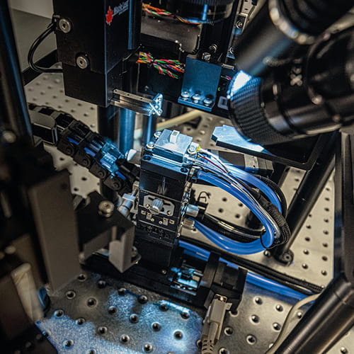
For Uxbridge, Mass.-based Iradion Laser, a maker of ceramic core CO2 lasers, LEAP’s reciprocal benefits are clear. The company is talking with the LEAP team about characterizing some parts to see if the parts deliver the expected results so Iradion can use them most efficiently. Having the facility in such close proximity saves time and money and has even opened the door to some possibilities Iradion hadn’t previously considered, including equipment they hadn’t had access to, says Talia Martin, a laser engineer at the company.
Julio Ramirez, director of research and development at Iradion, says students at LEAP could eventually turn into job-ready employees and collaborating with them at LEAP is beneficial to both sides. “We have to compete with many other companies and countries,” he says. “We can give students an idea of what they are going to face.” The growth, he says, happens on both sides and that spills over into the growing photonics ecosystem.
Cutting-edge Student Access
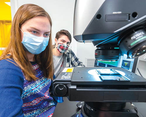
Students say seeing the academic and industry involvement informs their own work. “Some companies may give us some chips and ask us to measure them and report back on their performance,” says Jake Bouchard ’17, MS ’20, and current PhD candidate. “Others may want to come in and work on the chips themselves if they have classified projects or if they don’t want the technology they are working on to be known. Here, they gain access to millions of dollars of equipment and people who know how to use it, who can teach them how to use it, or who will do the work on the equipment for them.”
Bouchard says the ability to work on photonics research with in-depth training and access to complicated and highly sensitive equipment at LEAP is a rare opportunity for students and gives them a chance to connect their coursework with real-life use. “All the different applications of this technology drew me in,” he says. “Physics in general has so many varied applications—I call physics a ‘Swiss Army degree’—and photonics is such an up-and-coming application.” In his own work, Bouchard’s undergrad projects flipped a switch for him. “I started to look at my courses and ask, ‘what can I get out of this to apply directly to my research?’,” he says. “I would come across an application and know it was something I wanted to understand more.”
Bouchard’s been running tests on AIM-supplied chips and helping set up and use the LEAP equipment so he’ll be able to train students, researchers, and industry partners on proper use. He’s also been offering introductory LEAP tours to industry partners who are curious about the facility, what’s available for use, and how teams can help advance their business goals.
Working with such miniscule components requires some adjustment. “It’s not always the size,” Bouchard says. “It’s how fragile they are. These are the early stages, so the manufacturing process is expensive.” As he uses the test chips in a probe machine, he looks at how light works as it travels through the sides of the chip. “If you pick that up with tweezers and nick the side of it, the navigation of it is useless,” he says. “That’s the hardest learning curve—how to work with things that are so fragile.”
Morgan Kaler ’22 began her Interactive Qualifying Project (IQP) at LEAP just as the COVID pandemic shut down the university (a cancelled April 2020 LEAP ribbon-cutting ceremony will be rescheduled). Her goal is to chart how LEAP@WPI/QCC would evolve on its own, with the varied interests of different stakeholders, and within the larger LEAP ecosystem. Kaler says the recent pickup in activity offered insight into how LEAP will be used and gave her tech operations management experience that has helped standardize and measure LEAP’s forward process.
Watching Progress Materialize
LEAP removes one of the biggest barriers for photonics growth—access. “Opportunities to get your hands on equipment is not that common,” Bouchard says. “Only a few universities have LEAP labs or the equipment to train people so they can go out and get those jobs. It’s definitely cool to interact with these pieces of equipment.”
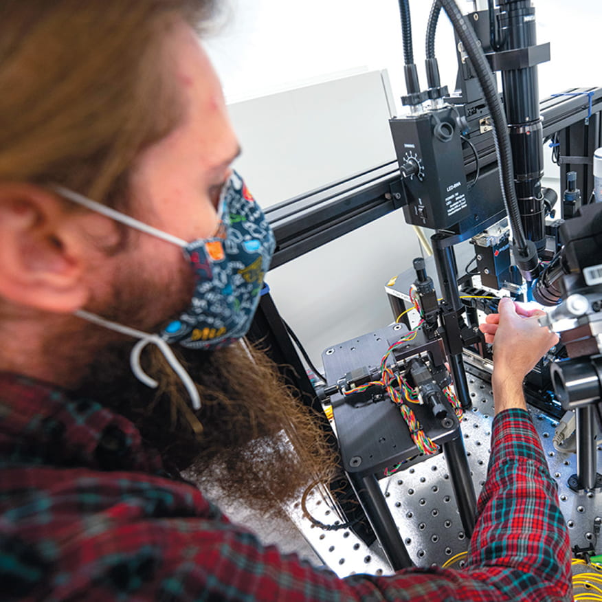
Only a few universities have LEAP labs or the equipment to train people so they can go out and get those jobs.
Jake Bouchard
The hands-on experience they get at LEAP is valuable, Kaler agrees, noting other students are already working at LEAP on IQPs and MQPs (Major Qualifying Projects) as well as other projects. “There are so many opportunities for students to get involved here,” Kaler says. “Whether it’s with doing research with a professor or by finding an IQP or MQP—right now, most of our users are students. As a student, it’s exciting to see my peers getting these kinds of opportunities.”
Kaler says LEAP offers exactly the experience WPI is known for. “In courses, you’re learning things that are theory-based, and you have to learn that to understand it,” she says, “but there’s not lots of room for the practical. LEAP gives an opportunity to build on what you’ve learned. You can say, ‘I’ve heard about this,’ and now you get to see how it works. One of the coolest things here is being able to see the collaborations and see the progress being made. Equipment is being used. Research is being done, and publications are coming out of it. The technology is advancing every day.”
Editor’s Note: WPI sadly notes the passing of Jacob Longacre, professor of electronics engineering technology & photonics at QCC, who died unexpectedly on Feb. 9, 2022, after the WPI Journal went to print. Read his obituary here.


